Difference between revisions of "Team:Bielefeld-CeBiTec/Hardware"

 
Line 88: Line 88:
 
The printing of metal nanoparticles allows for a quick prototyping and in combination with the special properties of metal nanoparticles very thin layers made of moderately heat stable materials becomes possible. </article>
 
The printing of metal nanoparticles allows for a quick prototyping and in combination with the special properties of metal nanoparticles very thin layers made of moderately heat stable materials becomes possible. </article>
 
<article>
 
<article>
To show that nanoparticles can indeed be made conductive at relatively low temperatures we ordered copper nanoparticles and either processed them further for creating a printable ink or used them directly for the production of conductive lines without further additives. </article><article>
+
To show that nanoparticles can indeed be made conductive at relatively low temperatures we ordered copper nanoparticles with a size of 40 nm and either processed them further for creating a printable ink or used them directly for the production of conductive lines without further additives.</article><article>
Since copper NP are known to oxidise when coming in contact with air all experiments needed to be done under N2 atmosphere.</article>
+
Since copper NP are known to oxidise when coming in contact with air all experiments needed to be done under N2 atmosphere. For that we used a plastic bag with inlets for the hands which was filled with N2 gas.</article>
  
 
<figure role="group"> <img class="figure hundred" src="https://static.igem.org/mediawiki/2018/7/7a/T--Bielefeld-CeBiTec--cg--N2Atmosphere.png">
 
<figure role="group"> <img class="figure hundred" src="https://static.igem.org/mediawiki/2018/7/7a/T--Bielefeld-CeBiTec--cg--N2Atmosphere.png">
Line 104: Line 104:
  
 
<article>
 
<article>
Beside the advantage of being easily processed into metallic inks and printed into any 2D shape the high surface energy of metal NP leads to a much lower melting point compared to metallic particles with micrometer scales. When NPs are heated to around 200°C they melt and fuse together to form a solid surface (Sunho Jeong et al., 2011).
+
Beside the advantage of being easily processed into metallic inks and printed into any 2D shape the high surface energy of metal NP leads to a much lower melting point compared to metallic particles with micrometer scales. When NPs are heated to around 200°C they melt and fuse together to form a solid surface (Sunho Jeong et al., 2011). Our experiments showed that 250°C was not enough to produce conductive structures with measurable conductivity. Instead we had to reach a temperature of 340°C to end up with conductive structures. This is remarkable when looking at the melting temperature of bulk copper which is as high as 1085°C. 
 
</article>
 
</article>
  
Line 114: Line 114:
 
</figure>
 
</figure>
 
<article>
 
<article>
For Cu-based nano inks, better conductivity is achieved when elemental Cu NPs are used. Copper oxide (CuO) NPs are formed when the NP are produced under aerobic conditions. CuO NPs have lower conductivity therefore a protective coating layer applied to the Cu NPs is often used to prevent oxidation prior to sintering.  
+
For Cu-based nano inks, better conductivity is achieved when elemental Cu NPs are used. Since copper oxide (CuO) NPs are formed when the NP are produced under aerobic conditions we tried to alwas avoide contact with air when working with the Cu NPs. CuO NPs have lower conductivity therefore a protective coating layer applied to the Cu NPs is often used to prevent oxidation prior to sintering.  
 
</article>
 
</article>
  
Line 121: Line 121:
 
<figure role="group"> <img class="figure hundred" src="https://static.igem.org/mediawiki/2018/5/52/T--Bielefeld-CeBiTec--cg--ConductiveCopper.jpg">
 
<figure role="group"> <img class="figure hundred" src="https://static.igem.org/mediawiki/2018/5/52/T--Bielefeld-CeBiTec--cg--ConductiveCopper.jpg">
 
<figcaption>
 
<figcaption>
<b>Figure 3:</b> Measuring the electrical resistance of our fragile copper nanoparticle prints. Display shows an resistance of 0.9 mOhm.
+
<b>Figure 3:</b> Measuring the electrical resistance of our copper nanoparticle prints. Display shows an resistance of 0.9 Megaohm.
 
</figcaption>
 
</figcaption>
 
</figure>
 
</figure>
 
<article>
 
<article>
The use of commercial inkjet printers for printing NP based ink allows for a very low hurdle of entry into the area of do-it-yourself (DIY) electronics (Yoshihiro Kawahara. et al., 2013). Our tests also showed that it is possible to use a commercially available household printers for printing different solvents which can be used to create copper inks. But the print head of standard printer easily clogs when copper nanoparticles (40 nm) are added to the ink. Therefore we recommend more traditional printing methods like screen printing for the low cost production of electronics made from metal nanoparticles. </article>
+
The use of commercial inkjet printers for printing NP based ink allows for a very low hurdle of entry into the area of do-it-yourself (DIY) electronics (Yoshihiro Kawahara. et al., 2013). Our tests also showed that it is possible to use a commercially available household printers for printing different solvents which can be used to create copper inks. Unfortunately the print head of standard printers easily clogs when copper nanoparticles (40 nm) are added to the ink. Therefore we recommend more traditional printing methods like screen printing for the low cost production of electronics made from metal nanoparticles. </article>
  
 
<figure role="group"> <img class="figure hundred" src="https://static.igem.org/mediawiki/2018/e/e4/T--Bielefeld-CeBiTec--cg--Cu_molten39.png">
 
<figure role="group"> <img class="figure hundred" src="https://static.igem.org/mediawiki/2018/e/e4/T--Bielefeld-CeBiTec--cg--Cu_molten39.png">

Latest revision as of 10:39, 6 December 2018

Hardware

Short Summary

We designed two hardware applications in accordance to our project. First, we constructed a cross-flow bioreactor designed to provide perfect conditions for the engineered cells to accumulate heavy metal ions. Parameters such as temperature, form and cell retention system were adjusted to design a cost-effective single-use reactor.
To further demonstrate the applicability of metal nanoparticles we demonstrated that copper nanoparticles can be processed into an ink which can be used for printing of electric circuits.

Printing Electronics

Printing electronics is a recent development whereby metal nanoparticles are mixed with organic solvents to form an ink that can be deposited in thin layers on various surfaces with inkjet printers or other printing techniques. After printing the nano ink gets reduced to elemental metal structures by either heating at relatively low temperatures or applying intense light. The printing of metal nanoparticles allows for a quick prototyping and in combination with the special properties of metal nanoparticles very thin layers made of moderately heat stable materials becomes possible.
To show that nanoparticles can indeed be made conductive at relatively low temperatures we ordered copper nanoparticles with a size of 40 nm and either processed them further for creating a printable ink or used them directly for the production of conductive lines without further additives.
Since copper NP are known to oxidise when coming in contact with air all experiments needed to be done under N2 atmosphere. For that we used a plastic bag with inlets for the hands which was filled with N2 gas.
Figure 1: Christoph working under a N2 atmosphere to protect the copper naoparticle from oxidising.
Only a few metals have a conductivity high enough to be practical for use in printed electronics. Copper (Cu) is cheap and widely available but has the disadvantage of oxidizing in ambient conditions. Cu also tends to agglomerate, which is unfavorable when used in NP ink.
Silver has the highest conductivity and does not oxidize making it a popular choice for flexible electronics. Gold on the other hand is very expensive but has the advantage of not reacting with biological systems.
Beside the advantage of being easily processed into metallic inks and printed into any 2D shape the high surface energy of metal NP leads to a much lower melting point compared to metallic particles with micrometer scales. When NPs are heated to around 200°C they melt and fuse together to form a solid surface (Sunho Jeong et al., 2011). Our experiments showed that 250°C was not enough to produce conductive structures with measurable conductivity. Instead we had to reach a temperature of 340°C to end up with conductive structures. This is remarkable when looking at the melting temperature of bulk copper which is as high as 1085°C.
Figure 2: Different probes made from copper ink or pure copper nanoparticles printed via the screen print technique and heated to 340°C.
For Cu-based nano inks, better conductivity is achieved when elemental Cu NPs are used. Since copper oxide (CuO) NPs are formed when the NP are produced under aerobic conditions we tried to alwas avoide contact with air when working with the Cu NPs. CuO NPs have lower conductivity therefore a protective coating layer applied to the Cu NPs is often used to prevent oxidation prior to sintering.
Figure 3: Measuring the electrical resistance of our copper nanoparticle prints. Display shows an resistance of 0.9 Megaohm.
The use of commercial inkjet printers for printing NP based ink allows for a very low hurdle of entry into the area of do-it-yourself (DIY) electronics (Yoshihiro Kawahara. et al., 2013). Our tests also showed that it is possible to use a commercially available household printers for printing different solvents which can be used to create copper inks. Unfortunately the print head of standard printers easily clogs when copper nanoparticles (40 nm) are added to the ink. Therefore we recommend more traditional printing methods like screen printing for the low cost production of electronics made from metal nanoparticles.
Figure 4: Our printed circuits under the TEM. The structure after heating the 40 nm particles to 340°C shows clusters of combined copper nanoparticles.

Design of a Cross-flow Bioreactor

We designed a cross-flow bioreactor perfectly adapted to filtering heavy metals out of mining drainage (MD) using genetically engineered Escherichia coli. Bacteria are retained in a reaction chamber while a large volume gets pumped through the chamber. The cells take up the heavy metals leading to an intracellular accumulation. The application was improved by user feedback and modeling and is now easy to run. It can easily be reconstructed by using the building plans we offer in our wiki. Furthermore, our device tackles the difficulty of applying GMOs to extract valuables out of large volumes and enables the safe application of GMOs outside the laboratory.
The task of scavenging metal ions from MD poses a great challenge to conventional cultivation strategies. Not only is the MD toxic to cells due to its elevated concentrations of sodium chloride and heavy metal ions like iron and copper. The shear amount of MD which has to be processed poses a problem in its own right. We tackle the toxic effects of heavy metals by our approach on anti-oxidants and anti-toxic measures leading to an improved cell viability.
To solve the problem of the large MD volume that has to be processed and, after our first assessment indicated that cultivating cells in such a large volume would be difficult and further complicate downstream processing (e.g. filtering of the biomass), we decided to construct a suitable hardware. Therefore, we designed a prototype for a customized cross-flow bioreactor adapted to the task of filtering large quantities of MD. The system comprises two core units: A reaction chamber for containing the cells (“reactor unit”) and a larger reservoir area providing mining drainage (“reservoir unit”) (figure 5).
Figure 5: Prototype of the first bioreactor.

The core units are connected by silicon tubes. The reactor unit is charged with genetically engineered Escherichia coli cells able to scavenge metal ions from the MD. Homogeneity is guaranteed by usage of a stir bar simulating a stirrer. The high concentration of bacterial cells is maintained by applying a filter membrane system to each port, preventing any living organism from the MD to contaminate the reaction unit or the E. coli cells to leave the reactor unit. Possible blocking of the membrane system because of filter cake could simply be prevented by reversing the flow direction. This is enabled by using a peristaltic pump with reversible pumping direction per tube. After the desired incubation time of the cells with the substrate medium, the cells in the reactor unit can be harvested by usage of the other two ports to the reactor unit.
However, after performing several tests we concluded that this prototype does not work the way it is intended to. Due to the speed of cells plugging the membrane filter system, it was not be possible to cycle the whole content of the reservoir unit through the system. The substrate medium was pumped in the reverse direction. However, since this event occurred rather quickly, only a small quantity of the MD was used for the incubation, leading to an incomplete process and limiting the yield. Therefore, we came up with a new design for the improvement of the desired cross-flow bioreactor. The basic design is maintained while substantial changes have been introduced to the reactor unit, in particular the filter membrane system.
Figure 6 Screenshot of the model on the improved bioreactor with adjustments for a settler system, a double jacket for isothermal cultivation and adjustments of the form to enable easier oxygenation.ments for a settler system, a double jacket for isothermal cultivation and adjustments of the form to enable easier oxygenation. The model was created using FreeCAD.

The filter system has been replaced by a favorable settler. This system is not only more cost-efficient in comparison to an expensive filter membrane system, it also enables the easy performable return of cells to the reactor unit without the risk of forming a filter cake. Cells leaving the reactor unit are intercepted by the settler based on the phenomenon of sedimentation. A glass hopper serves as a settler. If the cells sediment to the ground of the hopper, pressure is applied using a common syringe to pump sterile air into the settler system. The pressure applied by the syringe forces the accumulated biomass back into the reactor unit allowing to maximize the yield. The temperature of the reactor unit was adjusted to 37 °C using a double jacket plugged to a thermostat. Previously, the process occurred at room temperature. However, since E. coli exhibits the greatest activity at 37 °C, it is favorable to adjust the temperature to its needs. Control over the temperature is essential for process optimization. A conical form of the reactor unit improves the oxygenation of the culture. The whole system can be autoclaved.
In order to promote the thought of open source and public accessibility we provide the scientific community with a construction plan for 3D printing both reactor units using the freeware FreeCAD. The production takes approximately eight hours using a 3D printer. Since the favored printing material polylactic acid (PLA) costs around 0.5 USD per cm3, reconstructing the reactor unit is cheap. Several components of the system can be produced using PLA although using glass is possible as well. Cell retainment in the reactor unit saves time and reduces costs as working procedures to separate the cells from the medium become no longer necessary. Silicon tubes can be acquired for 0.88 USD per meter, peristaltic pumps for less than 177 USD, yielding a total cost of less than 360 USD for the complete reactor.
Below we offer the files for the freeware FreeCAD which are necessary to reconstruct our reactor and the corresponding components.
Figure 7 Screenshot of the model on the improved bioreactor with adjustments for a settler system, a double jacket for isothermal cultivation and adjustments of the form to enable easier oxygenation.ments for a settler system, a double jacket for isothermal cultivation and adjustments of the form to enable easier oxygenation. The model was created using FreeCAD.
Figure 8 Screenshot of the model on the designed settler. The model was created using FreeCAD.
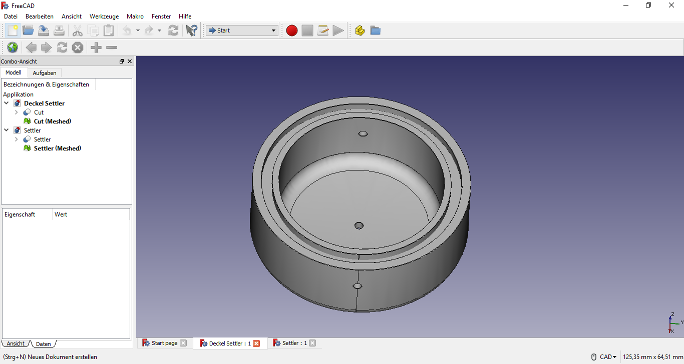
Figure 9 Screenshot of the model on the lid for the settler. The model was created using FreeCAD.
Click here to download the files.

Raut, N. C., & Al-Shamery, K. (2018). Inkjet printing metals on flexible materials for plastic and paper electronics. Journal of Materials Chemistry C, 6(7), 1618-1641.